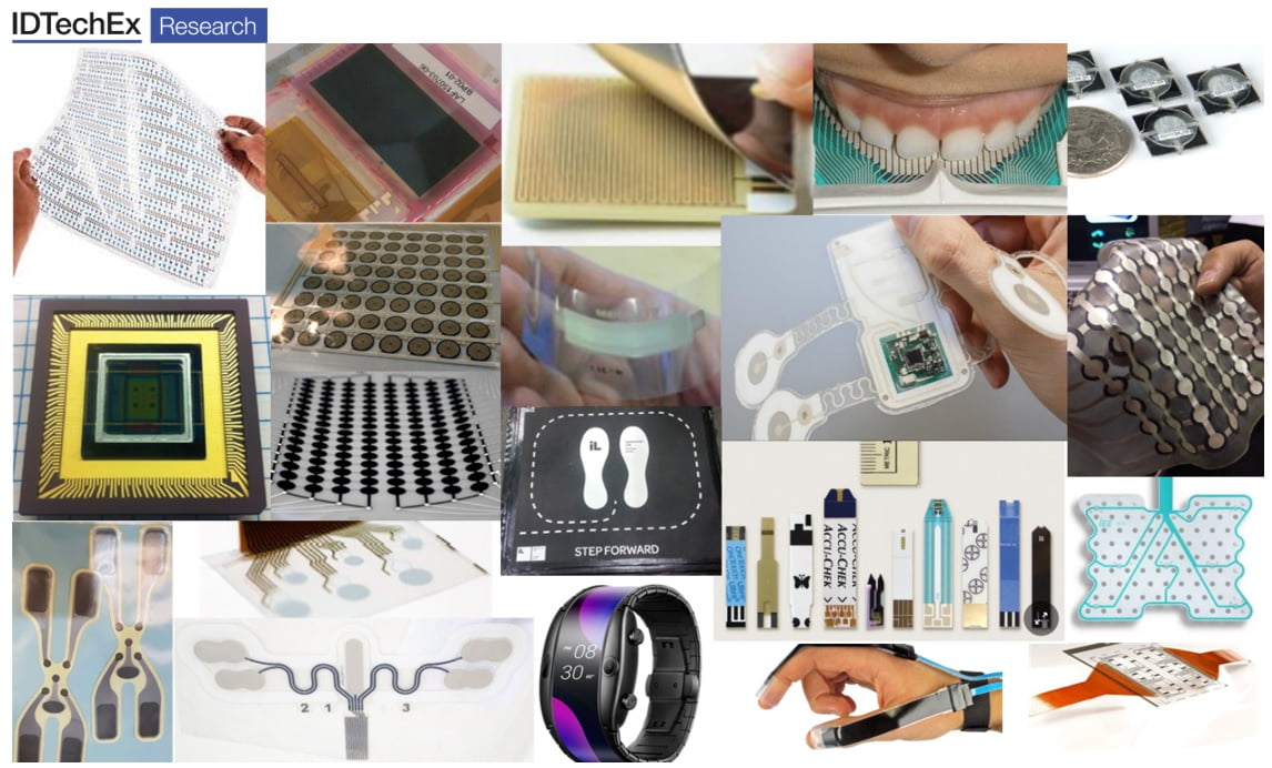
Asked to picture a printed sensor, you might well imagine a paper test strip for measuring blood glucose concentration. After all, such test strips comprise the majority of the printed sensor market, with billions used each year by diabetics around the world. However, this ubiquitous application masks a highly complex, fragmented and in some cases rapidly growing market that spans applications ranging from image sensing to wearable electrodes.
Q1 2020 hedge fund letters, conferences and more
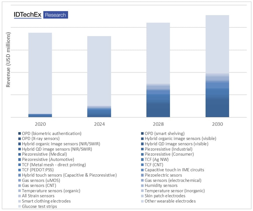
The new IDTechEx report, “Printed and Flexible Sensors 2020-2030: Technologies, Players, Forecasts”, covers the entire printed and flexible sensor landscape. Collectively, printed sensors constitute the largest printed electronics market, which IDTechEx forecasts to reach $4.5 billion by 2030 despite the sustained displacement of printed glucose test strips by continuous glucose monitoring (CGM). Market growth is therefore enabled by the rise of many new applications and technologies. Specifically, this IDTechEx report covers:
- Large area image sensors
- Hybrid QD/Organic-on-CMOS image sensors
- Hybrid sensors for SWIR imaging
- Piezoresistive sensors
- Piezoelectric sensors
- Temperature sensors
- Capacitive strain sensors
- ITO alternatives for capacitive touch sensors
- Gas and humidity sensors
- Biosensors
- Printed electrodes for skin patches and e-textiles
Within this diverse application space some sensors comprise a very simple structure with only a few layers, whilst others are much more complex and require the deposition of multiple layers and sophisticated, innovative materials. Some sensors are sheet-to-sheet screen printed, whereas others are made using continuous roll-to-roll printing. The majority are on low-cost flexible large-area substrates, but some, however, are to be found atop CMOS devices or various textile substrates.
Each sensor category seeks to offer a distinct value proposition over the incumbent technology, with a specific motivation for using printing as a manufacturing methodology. Furthermore, each has its different technological and commercial challenges on route to widespread adoption. The new IDTechEx report, “Printed and Flexible Sensors 2020-2030: Technologies, Players, Forecasts”, comprehensively evaluates the technology underpinning each printed sensor category, along with the players, market positioning and commercial prospects. IDTechEx also develops highly granulated 10-year market forecasts, delineated by technology and application. Here, the underpinning technology, market landscape and commercial prospects of each sensor are briefly reviewed, demonstrating the diversity of this rapidly growing sector.
Printed and flexible sensors comprise a wide range of technologies and applications, including organic and hybrid photodetectors, piezoresistive and piezoelectric pressure sensors, stretchable strain sensors, temperature sensors, printed electrodes for skin patches, biosensors, gas sensors, humidity sensors, and ITO alternatives for capacitive touch sensors.
Hybrid Image Sensors
Hybrid image sensors are an especially promising category. They comprise of a thin film (a few 100 nm) of either an organic semiconductor or quantum dots printed over a silicon readout circuit. They offer three distinct value propositions over the incumbent silicon CMOS detectors: a tuneable bandgap to enable NIR and SWIR imaging at much longer wavelengths, voltage-dependent sensitivity that enables spatially-variable neutral density filter, and more rapid charge collection that facilitates a global rather than rolling shutter.
Critically, hybrid image sensors can be manufactured using repurposed CMOS lines, substantially reducing capital requirements, and facilitating more rapid adoption. The OPD-on-CMOS technology is set to be launched imminently in broadcast cameras, while the QD-on-CMOS technology is already commercially available and will transition to higher-power out-door applications as the thermal and light flux stability of the material system evolves over time. Therefore, the technology can migrate from indoor low-light inspection to outdoor applications such as SWIR imaging for autonomous vehicles.
This disruptive hybrid approach meets genuine market needs, demonstrating that integrating printable, functional materials with standard technology and manufacturing methods can enable substantial performance improvements while lowering adoption barriers. To learn more about the current and future status of all technology options and the business landscape, along with commercial adoption roadmaps, in this exciting and rapidly developing sector please consult this new report.
Large Area Image Sensors
Large area image sensors based on printed organic photodiodes (OPDs) are an innovative technology, representing a complete change from the conventional CMOS-based image detection and going beyond what other large-area image sensors technologies can offer. The technology has two related value propositions: it is flexible and lightweight, unlike large area a-Si image detectors, and in principle it can be printed rapidly at low cost using continuous manufacturing methods.
However, today there are very few manufacturers, and these are mainly targeting biometric sensing as a relatively high value application, thus enabling them to avoid competing with CMOS. In one proposed application, large area under-the-screen image sensors enable 4 fingerprints to be imaged simultaneously, in contrast to the incumbent technology that either images a single finger or requires a complex optical system to image a large area.
While technically impressive, large area image sensing appears to be largely driven by pushing the technology rather than maker need. It is questionable whether this capability represents a sufficient advance over incumbent methods to overcome the entry barrier to adoption, especially as fingerprint recognition must compete with incumbent methods.
Piezoresistive Sensors
Printed piezoresistive force sensors are a longstanding application, widely used today in car occupancy sensors, musical instruments, industrial equipment, and some medical devices. While these markets are somewhat commoditized, the sector is innovating to access new, differentiated, higher value applications.
One example is 3D touch panels that can measure applied force as a function position, thus enabling the recognition of complex HMI gestures than the incumbent capacitive touch panels. Suppliers are continuing to target phones, computer gaming and automotive interiors. Other innovations include hybrid capacitive/piezoresistive sensor arrays that detect proximity but require a firm push to actuate, piezoresistive handles as a safety device for power tools, and manufacturing via roll-to-roll processing.
The challenge for differentiating piezoresistive sensors is that many applications do not require sophisticated functionality such as 3D touch or proximity sensing. Furthermore, the revenue streams can widely fluctuate with the various product cycles, requiring very active development of the application pipeline. The relatively low technology complexity can also mean that barriers to entry and the value capture are low. This is convincing some to go higher up in the value chain, offering fully integrated solutions.
Piezoelectric Sensors
Piezoelectric sensors generate a voltage in response to an applied force, rather than changing their resistance. While, like piezoresistive sensors, they can be used for force sensing, they are more expensive to manufacture and less straightforward to integrate. As such, manufacturers are primarily targeting applications that utilize their unique capabilities, specifically their sensitivity to high frequency vibrations.
In this IDTechEx report, two printable piezoelectric materials are covered: polymers and inorganic-containing composites. The former have seen greater commercial uptake, but both are still under development. The commercial difficulty for printed piezoelectric sensors is that their capabilities lie midway between two simple established technologies: Affordable piezoresistive pressure sensors, and sensitive, rigid ceramic piezoelectric sensors. As such, piezoelectric sensing applications are rather niche, unless the technological readiness level of energy harvesting dramatically increases to enable self-powered sensors.
A better value proposition, where these materials have unique capability, is for flexible high frequency actuators (i.e. wearable ultrasound generators for medical therapeutics). To learn more about the technologies, players, and market positioning of piezoelectric sensors, please see the IDTechEx report “Printed and Flexible Sensors 2020-2030: Technologies, Players, Forecasts”.
ITO Alternatives for Capacitive Touch
The development of ITO alternatives has long been motivated by ITO’s shortcomings: limited flexibility, limited conductivity, and exposure to the indium price and supply chain. Emerging alternatives include silver nanowires, carbon nanotubes and various forms of metal mesh films. These alternatives offer lower sheet resistance, higher flexibility, and sometimes even stretchability for 3D-shaped molded applications.
Interestingly, more alternatives are printed, or solution processed. Ag nanowires and carbon nanotubes can be solution coated, whilst advances in hybrid or direct printing of fine-feature lines has enabled partially or fully printed metal mesh films with linewidths below 3 um.
ITO remains the incumbent transparent conductive material used in touch screen, despite nearly two-decades of attempts to unseat it. This displacement was partly hampered by technical issues such as stability or haze and partly by commercial reasons. In particular, the dominant strategy of market share protection pursued by ITO suppliers and supported by the previous fall in indium prices drove a tough consolidation in the market.
Nonetheless, these alternatives are finally finding market in flexible or 3D shaped objects, in large-area multi-touch capacitive touch screens, and even nowadays sometimes in lower cost touch screens. This IDTechEx report includes a detailed technical and commercial benchmarking of the different technology options, an application roadmap, and market forecasts segmented by Ag nanowires, carbon nanotubes, ITO film and various forms of hybrid or printed metal mesh. The technologies and market for both metallic and transparent conductive inks is extensively discussed in the recently updated IDTechEx report, “Conductive Ink Markets 2020-2030: Forecasts, Technologies, Players”.
Capacitive Strain Sensors
Various partially or fully printed stretchable strain sensors have been developed and commercialized over the years. Basic technology demonstration has proved relatively easy, but not every supplier has succeeded in transitioning to large-volume capability with at lower costs.
The main challenge has been that flexible strain sensors are generally not replacing an existing product, meaning that completely new markets need to be developed. To address this challenge and to capture more value, many suppliers offer vertically integrated ‘solutions’.
After years of development opportunities in industrial displacement sensing, in wearable electronics, and in continuous patient monitoring are now emerging.
Temperature Sensors
Printing can also be used to create temperature sensors, using either a composite ink with silicon nanoparticles or carbon nanotubes. Given that temperature measurement requires good thermal contact sensors based on conformal substrates might seem to offer a clear value proposition.
Their main challenge is the low cost, light weight, and ubiquity of very mature solutions such as thermistors and resistive temperature detectors. These can be deployed with a flexible thermal conductor, thus somewhat nullifying the value proposition of printed temperature sensors. As such, they are best suited to applications that require spatial resolution using conformal array, such as monitoring skin complaints. Monitoring the temperature of batteries in electric vehicles is another possible application, but one that has yet to be widely adopted and could arguably be achieved with multiple thermistors.
Gas and Humidity Sensors
Gas and humidity sensors can also be printed, although at present most are made from ceramics rather than organic material. Some of these ceramics are printed as a ‘thick film’ with very high curing temperatures, rendering them incompatible with flexible substrates. Emerging approaches are based around functionalized carbon nanotubes and other organic semiconductors. Multiple sensors with slightly different properties can be combined to form an ‘electronic nose’, with their composite output exhibiting a different ‘fingerprint’ for each analyte.
Gas sensors are already used in many industrial contexts and are likely to be increasingly adopted as concern about air pollution grows. Unlike some sectors, there is substantial scope for differentiation by sensitivity and analyte, leading to a fragmented market. Another promising long-term application in which printed gas sensors offer unique capability is directly printing onto food packaging to measure food degradation. However, this will likely require the development of flexible hybrid electronics to make such capability cost-effective via continuous manufacturing, along with the development of enabling technologies such as flexible ICs. Flexible hybrid electronics are discussed in more detail in the IDTechEx report, “Flexible Hybrid Electronics 2020-2030: Applications, Challenges, Innovations and Forecasts”.
Biosensors
The largest category of printed sensors by revenue and volume is printed biosensors, dominated by glucose test strips. The annual demand is in the billions. However, use is gradually declining due to the adoption of convenient continuous glucose monitoring, a trend that will continue to grow. In parallel, there have been significant price pressures and commoditization as regulators have sought to supress the test prices and in doing so eroded the margins. Despite all this, this remains the largest volume and revenue business in the printed and flexible sensor landscape. Importantly, printed biosensors are not constrained to glucose sensing and an array of other sensors are emerging.
Wearable Electrodes
Today, most medial electrodes comprise a metal snap fastening with an electrolytic gel, but these can only be used for short periods. For continuous monitoring, printed electrodes are gradually being adopted into skin patches, since they last longer, can be integrated into a product together with conductive interconnects (also printed) and are flexible. Wearable electrodes are also well suited to fitness context and have been integrated into e-textiles to monitor heart rate in a comfortable way. Both medical and fitness applications of printed wearable electrodes are likely to increase as the software for continuous monitoring develops thus creating greater demand, although the durability in e-textiles remains a concern for consumers. Skin patches and e-textiles are discussed more comprehensively in the IDTechEx reports: “Electronic Skin Patches 2020-2030” and “E-textiles and Smart Clothing 2020-2030: Technologies, Markets and Players”.
The post Printed Sensors: Emerging Applications Outweigh Test Strip Decline appeared first on ValueWalk.


